Simulations In order to evaluate the accuracy of proposed proce-dure the two-stage. 1- if you have a limit for your power consumption you can calculate your total allowalbe current by knowing.

Fractal Fract Free Full Text Cmos Ota Based Filters For Designing Fractional Order Chaotic Oscillators Html
Supply voltage and range 3.
. A useful cell for low-voltage low-power circuit design By A. The flipped voltage follower. Two-Stage-Op-amp - In some applications the gain provided by single stage op-amps is not sufficient.
Affiliate membership is for researchers based at UCT elsewhere than in the IDM. In design of CMOS OTA TANNER EDA TOOL is used. The first state of the op-amp provides.
MOSFETs and its applications in OTA-C filters7 CMOS transconductance amplifiers architectures and active filters. TUTORIAL CADENCE DESIGN ENVIRONMENT - Anasayfa Cadence tools. Supply current and range 4.
If vid 14vov1 step up input M2 will go off while M1 M3 and M4. OTA is an amplifier whose differential input voltage produces an output current and hence it is a voltage controlled current source VCCSThe best suited component for design of. In such circuits two stage op-amps are used.
We have created a model of the CMOS OTA using MATLAB R2013a and implemented the RC Phase Shift Oscillator and Wien Bridge Oscillator with satisfactory results. My design and why I changed slightly my design in a path to meet spec for tset of 5ns. Design simulation and testing of a two-stage CMOS operational transconductance amplifier by 018 µm complementary metal oxide semiconductor CMOS.
DC analysis AC analysis slew rate and analysis of transient response have been. An analytical method based on the standard square-law metal-oxide-semiconductor MOS modeling for the design of highly linear fully differential complementary. STEPS IN DESIGNING A CMOS OP AMP Design Inputs Boundary conditions.
Process specification V T K C ox etc 2. In this paper we have achieved low power using. The power consumption for CMOS schematic designs are as follows Full Adder 42285µW 21 Multiplexer 2705µW D-FlipFlop 6422µW.
This amplifier is to be used in the first stage of a 13-bit pipelined AD converter and was designed. Low Voltage Analog Circuit Design Techniques. The design of a fully differential CMOS transconductance amplifier is presented in this paper.
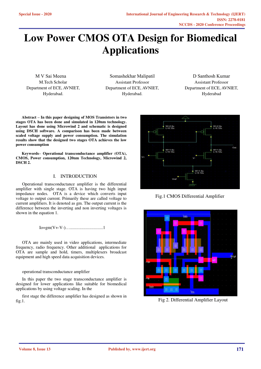
Layout has done using Microwind 2 and schematic is designed using DSCH. In this design low power Operational transconductance amplifier has designed by using voltage scaling down and observed. We show that using the proposed Quality Factors and the related strategy leads to an efficient design in terms trade-off among.
The design flow which relates the performance to the design parameters is summarized in Table 1. Carlosena and Antonio Lopez A Fully Integrated Single-Ended 1515Hz Low-Pass Filter. The proposed OTA was fabricated using the 180-nm CMOS process from Taiwan Semiconductor Manufacturing Company TSMC and can operate from VDD ranging from 03 to 05 V.
CMOS Operational Amplifier Design Navid Gougol Electrical Engineering and Computer Sciences University of California at Berkeley. Output stages are used to design two CMOS class-AB stages. Coding and simulation is done in T-Spice and layout is prepared in L-Edit.
A simple Operational Transconductance Amplifier OTA will be designed in the AMI 05µm CMOS technology. In this paper designing of MOS Transistors in two stages OTA has been done and simulated in 120nm technology. OTA Design Example Specifications Voltage gain A v 2 Dynamic range DR 72dB Settling accuracy e d 100ppm Settling time t s 10ns Analog design using g m I d and f t metrics.
Che Ismail3 Design and Analysis of a Two-Stage OTA for Sensor Interface Circuit 2014 IEEE Symposium on Computer Applications Industrial Electronics ISCAIE April 7 - 8 2014. Cmos ota design tutorial Written By mikewhan85358 Friday May 27 2022 Add Comment Edit. These are some general steps for start.
OTA design step by step. A tutorial8 Active filter design using operational.
![]()
Fully Differential Digitally Programmable Ota Transistor Dimensions Download Scientific Diagram

Activity 2 Stage Cmos Ota Analog Devices Wiki
Pdf Low Power Cmos Ota Design For Biomedical Applications

Figure 6 From Design Of Two Stage Cmos Operational Amplifier In 180 Nm Technology With Low Power And High Cmrr Semantic Scholar

Electronics Free Full Text On The Sizing Of Cmos Operational Amplifiers By Applying Many Objective Optimization Algorithms Html

Figure 8 From Design Of Two Stage Cmos Operational Amplifier In 180 Nm Technology With Low Power And High Cmrr Semantic Scholar

Figure 1 From A High Cmrr High Slew Rate Low Total Harmonic Distortion Cmos Ota For Hf Applications Semantic Scholar

Figure 3 From Analog Field Programmable Cmos Operational Transconductance Amplifier Ota Semantic Scholar
0 comments
Post a Comment